Carry-skip adder
Arithmetic logic circuit
| Part of a series on | |||||||
| Arithmetic logic circuits | |||||||
|---|---|---|---|---|---|---|---|
| Quick navigation | |||||||
| Theory
| |||||||
| Components
| |||||||
| Categories
| |||||||
| See also | |||||||
|
A carry-skip adder[nb 1] (also known as a carry-bypass adder) is an adder implementation that improves on the delay of a ripple-carry adder with little effort compared to other adders. The improvement of the worst-case delay is achieved by using several carry-skip adders to form a block-carry-skip adder.
Unlike other fast adders, carry-skip adder performance is increased with only some of the combinations of input bits. This means, speed improvement is only probabilistic.
Single carry-skip adder
The worst case for a simple one level ripple-carry adder occurs, when the propagate-condition[1] is true for each digit pair . Then the carry-in ripples through the -bit adder and appears as the carry-out after .


For each operand input bit pair the propagate-conditions are determined using an XOR-gate. When all propagate-conditions are true, then the carry-in bit determines the carry-out bit.


The n-bit-carry-skip adder consists of a n-bit-carry-ripple-chain, a n-input AND-gate and one multiplexer. Each propagate bit , that is provided by the carry-ripple-chain is connected to the n-input AND-gate. The resulting bit is used as the select bit of a multiplexer that switches either the last carry-bit or the carry-in to the carry-out signal .


![{\displaystyle s=p_{n-1}\wedge p_{n-2}\wedge \dots \wedge p_{1}\wedge p_{0}=p_{[0:n-1]}}](https://wikimedia.org/api/rest_v1/media/math/render/svg/2b3605f5ec48e20ef15e209c165e78fb6a96ceef)
This greatly reduces the latency of the adder through its critical path, since the carry bit for each block can now "skip" over blocks with a group propagate signal set to logic 1 (as opposed to a long ripple-carry chain, which would require the carry to ripple through each bit in the adder). The number of inputs of the AND-gate is equal to the width of the adder. For a large width, this becomes impractical and leads to additional delays, because the AND-gate has to be built as a tree. A good width is achieved, when the sum-logic has the same depth like the n-input AND-gate and the multiplexer.

Performance
The critical path of a carry-skip-adder begins at the first full-adder, passes through all adders and ends at the sum-bit . Carry-skip-adders are chained (see block-carry-skip-adders) to reduce the overall critical path, since a single -bit carry-skip-adder has no real speed benefit compared to a -bit ripple-carry adder.


The skip-logic consists of a -input AND-gate and one multiplexer.


As the propagate signals are computed in parallel and are early available, the critical path for the skip logic in a carry-skip adder consists only of the delay imposed by the multiplexer (conditional skip).
- .

Block carry-skip adders
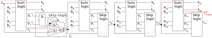
Block-carry-skip adders are composed of a number of carry-skip adders. There are two types of block-carry-skip adders The two operands and are split in blocks of bits.


- Why are block-carry-skip-adders used?
- Should the block-size be constant or variable?
- Fixed block width vs. variable block width
Fixed size block-carry-skip adders
Fixed size block-carry-skip adders split the bits of the input bits into blocks of bits each, resulting in blocks. The critical path consists of the ripple path and the skip element of the first block, the skip paths that are enclosed between the first and the last block, and finally the ripple-path of the last block.

![{\displaystyle T_{FCSA}(n)=T_{CRA_{[0:c_{out}]}}(m)+T_{CSK}+(k-2)\cdot T_{CSK}+T_{CRA}(m)=3D+m\cdot 2D+(k-1)\cdot 2D+(m+2)2D=(2m+k)\cdot 2D+5D}](https://wikimedia.org/api/rest_v1/media/math/render/svg/8419066be5bc3bbe10b5b9af3ecbc032b46ff9a1)
The optimal block size for a given adder width n is derived by equating to 0


Only positive block sizes are realizable

Variable size block-carry-skip adders (VBA, Oklobdzija-Barnes)[2]
The performance can be improved, i.e. all carries propagated more quickly by varying the block sizes. Accordingly the initial blocks of the adder are made smaller so as to quickly detect carry generates that must be propagated the furthers, the middle blocks are made larger because they are not the problem case, and then the most significant blocks are again made smaller so that the late arriving carry inputs can be processed quickly.
Multilevel carry-skip adders
By using additional skip-blocks in an additional layer, the block-propagate signals are further summarized and used to perform larger skips:
![{\displaystyle p_{[i:i+3]}}](https://wikimedia.org/api/rest_v1/media/math/render/svg/41aeb6cd41eb4fc55e591ca897a99e81b1e89ea2)
![{\displaystyle p_{[i:i+15]}=p_{[i:i+3]}\wedge p_{[i+4:i+7]}\wedge p_{[i+8:i+11]}\wedge p_{[i+12:i+15]}}](https://wikimedia.org/api/rest_v1/media/math/render/svg/0dea9b3e7dec8d85e82bcecec0da5ebd1b856c5d)
Thus making the adder even faster.
Carry-skip optimization
The problem of determining the block sizes and number of levels required to make the physically fastest carry-skip adder is known as the 'carry-skip adder optimization problem'. This problem is made complex by the fact that a carry-skip adders are implemented with physical devices whose size and other parameters also affects addition time.
The carry-skip optimization problem for variable block sizes and multiple levels for an arbitrary device process node was solved by Oklobdzija and Barnes at IBM and published in 1985.
Implementation overview
Breaking this down into more specific terms, in order to build a 4-bit carry-bypass adder, 6 full adders would be needed. The input buses would be a 4-bit A and a 4-bit B, with a carry-in (CIN) signal. The output would be a 4-bit bus X and a carry-out signal (COUT).
The first two full adders would add the first two bits together. The carry-out signal from the second full adder ()would drive the select signal for three 2 to 1 multiplexers. The second set of 2 full adders would add the last two bits assuming is a logical 0. And the final set of full adders would assume that is a logical 1.

The multiplexers then control which output signal is used for COUT, and .


Notes
- ^ Carry-skip adder is often abbreviated as CSA, however, this can be confused with carry-save adder.
References
- ^ Parhami, Behrooz (2000). Computer arithmetic: Algorithms and Hardware Designs. Oxford University Press. p. 108. ISBN 0-19-512583-5.
- ^ V. G. Oklobdzija and E. R. Barnes, "Some Optimal Schemes For ALU Implementation In VLSI Technology", Proceedings of the 7th Symposium on Computer Arithmetic ARITH-7, pp. 2-8. Reprinted in Computer Arithmetic, E. E. Swartzlander, (editor), Vol. II, pp. 137-142, 1985.
External links
- Explanation for critical path of the variable-skip adder


